
![]()
|
|
|
|
|
|
Intusoft
Newsletter Issue #55, March 1999
Copyright
©2002 Intusoft, All Rights Reserved
New Magnetics Designer v4.0 Get Finite Elements Analysis Features
Intusoft is releasing a new version of its popular transformer and inductor design program, Magnetics Designer. The new version 4.0 represents a significant breakthrough in terms of performance and new features. A major enhancement includes the ability to handle sector winding configurations for high voltage designs. A new "Bobbin tab" allows you to see the winding structure (Figure 1), as well as export the structure in the DXF file format. New 2D Finite Element Analysis (FEA) algorithms produce magnetic field maps that describe the winding magnetic field. The FEA solutions enable calculation of the AC losses for sector wound geometries.
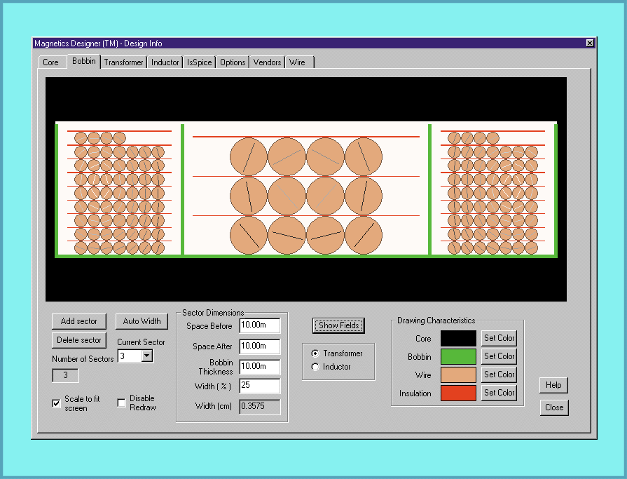
Figure 1, The new Magnetics Designer v4.0 adds sector winding
capabilities, winding structure image (shown above), DXF output
and FEA algorithms.
Data entry is eased with the addition of a Design Wizard (Figure 2). An expanded winding screen gives you more per winding information such as current density and winding weight (Figure 3). Silver and aluminum wire types are now supported, along with a core database that contains more than 7,000 cores.
Program Overview
Magnetics Designer synthesizes all types of transformers and inductors. Typical applications include high power transformers for aerospace and industrial power levels, subminiature planar magnetics and general switched mode power supply design. Virtually any single phase, layer or sector wound inductor or transformer, from 10Hz to over 5MHz, can be synthesized with Magnetics Designer. Magnetics Designer is different than other FEA based analysis tools. It actually selects the core geometry and synthesizes the winding structure for you, making you dramatically more productive. You do not have to draw anything or specify any physical design characteristics other than the core family, material and type of wire (formvar, square, Litz, foil, pcb trace) you want to use.
What Makes Magnetics Designer Unique
Magnetics Designer performs synthesis as well as analysis of transformers and inductors.
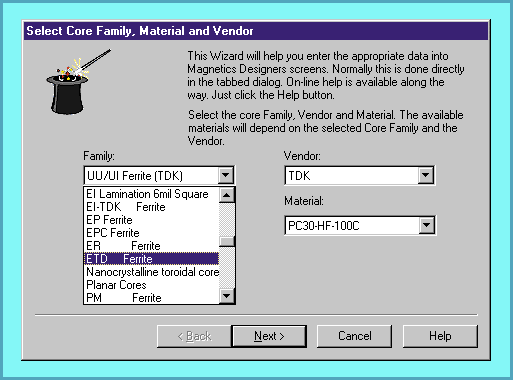
Figure 2, The new Design Wizard helps lead you through entry
of the required parameters: Core Family, Material, Wire Type,
Operating Frequency, Voltage/Current per winding, and allowed
Temperature rise. Entering design specifications is a simple matter.
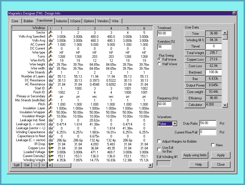
Figure 3, The expanded Transformer screen displays more
winding information. Major enhancements include the ability to
handle split bobbin configurations and more versatile specification
of the current waveform. A Fourier series is computed for the
specified pulse waveform duty cycle and rise/fall time. New Finite
Element Analysis (FEA) algorithms give you more accurate calculation
of the AC losses.
Classical design methods rely on home-grown software programs that are patched together, or "build and test" iterations that are exercised until the appropriate behavior of the prototype component is achieved. Magnetics Designer eliminates these costly design methodologies by accurately synthesizing and analyzing the magnetic structure for you.
Magnetics Designer achieves significant gains in productivity by combining advanced analytical algorithms and 2D FEA techniques in a single, easy-to-use software tool. Initially, multi-parameter optimizations are employed to handle the design variable trade-offs (about 10,000 optimization passes per design). Finite element calculations are performed after the speedier analytical optimization algorithms. Tools which use FEA as the primary solution path can't perform the design variable trade-offs efficiently due to long run time constraints. Thus, the user is forced to choose the specific core geometry and winding structure. This is a major drawback. Magnetics Designer, on the other hand, does this for you.
Since the multi-parameter optimization algorithms are fast, the user can compare designs quickly and easily. The user can change more than 20 parameters such as allowed temperature rise, allowed window fill, number of turns, wire gauge and type, bobbin margins, number of parallel strands, gap length, layer insulation thickness, wrapper thickness, and end margin lengths. The program allows the user to split, move, and interleave windings and set variable size sectors.
The result is a tool that generates an optimized design with accurate calculations of all key performance characteristics from a simple list of electrical, mechanical, and thermal specifications. Designers can consider various geometry, material and winding strategies without actually building the component, thereby ensuring a low cost, efficient design.
More information, application notes, a FAQ, and a demonstration version of Magnetics Designer are available on Intusoft's web site.
The "Power Specialist's App Note Book" contains over 35 technical articles on power supply design and power electronics modeling. The papers cover a wide range of topics including: SMPS design, magnetics modeling, signal generator modeling, power semiconductor modeling, and power supply testing. Many useful examples and modeling tips are included, as well as detailed discussions of key power supply design issues.
The book is posted on the Intusoft web site in PDF format. It can be downloaded at no charge.
The ICAP/4 simulation system contains many unique features. If you have used, or are using other SPICE packages, you may not be familiar with them. In this installment we discuss Automated Measurements.
The traditional post analysis methods for SPICE output data are analogous to using an oscilloscope. You select and display a waveform from the list of saved data, move cursors on the waveform and make your measurement (peak-peak, max, min, etc.) This process, while simple, is too time consuming when dozens of waveforms must be analyzed and hundreds of measurements must be made. This is the case when performing design validation, failure analysis or test program development.
Fortunately, ICAP/4 includes a new paradigm for waveform analysis. It's called Automated Measure-ments. The process is simple. Using a series of "Wizard" dialogs (Figure 4), you setup the desired measurements. Virtually any circuit quantity can be recorded, including DC, rise/fall time, prop. delay and triggered measurements on voltages, currents, or power dissipations. You do not have to write any scripts or do any programming to setup the measurements.
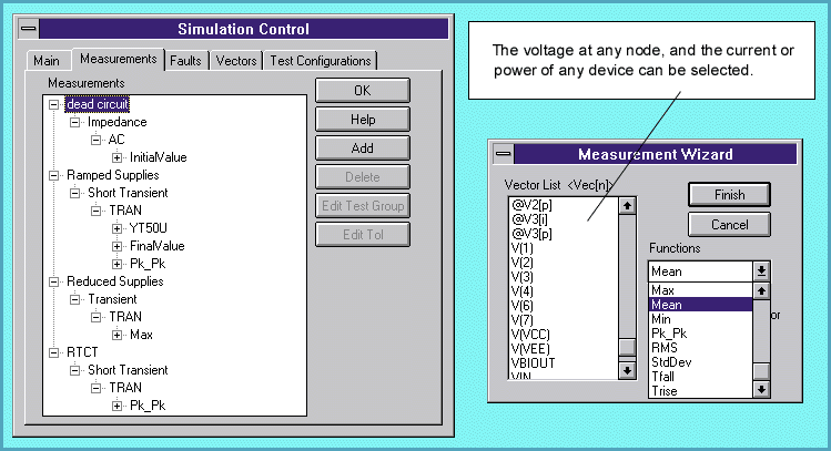
Figure 4, ICAP/4 allows you to setup several circuit variations with different topologies and part values (left). You can then assign as many automatic measurements as you want using a graphical Wizard approach (right).
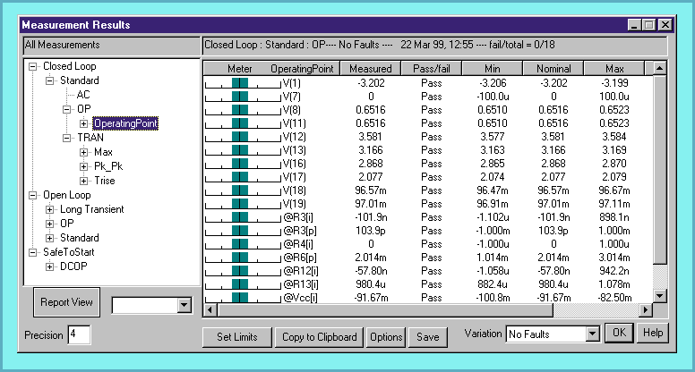
Figure 5, The measurements are recorded automatically after
the simulation is complete. The nominal measurement performance,
shown above, can be viewed after setting the min/max limit boundaries
for each measurement.
The measurements are automatically performed by IsSpice4 each time a simulation is run, and the results are compiled into a report (Figure 5). You can set limits or stress alarms for each measurement. The report will tell you how any circuit change (stimulus, part value, model parameter, etc.) affects your design (Figure 6). The best part is that the data gathering, calculation of the measured quantity, and report generation are completely automatic and transparent to the user. No user interaction is needed to process the measurements!
Why is this feature important? It gives you a general data analysis framework that is far more productive than the traditional methods of waveform analysis.
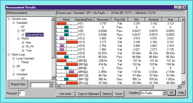
Figure 6, The measurements (Measured column) are recorded
automatically after the simulation is complete, and are compared
with the nominal values. Variations against the test limits can
be easily seen using the Meter column.
by Karl Heinz Muller
Inverters, as defined here, convert DC power into AC power. They are widely used in single and three phase industrial applications. To limit heat dissipation, efficiencies greater than 90% are of primary interest, especially in the kilowatt range. Power transistors therefore, operate as switches, generating a square wave voltage at the output terminals as shown in the 400Hz-Inverter in Figure 7. Many types of equipment operate satisfactorily on a square wave supply voltage, but in some instances, a filter at the output is necessary (as shown in Figure 9) to suppress objectionable harmonics.
The power MOSFETs work in a push-pull mode. No net direct current flows through the center-tapped transformer, thereby reducing its size and weight. In a similar manner, all even-order harmonics are cancelled by symmetry (Figure 8). Stabilization of the output voltage is accomplished by a feedback loop that regulates the pulse width of the gate waveforms for the power MOSFETs. Figure 8 shows that with increasing DC-supply voltage, V0, the pulse width of output voltage decreases accordingly, keeping its RMS value at a constant level.
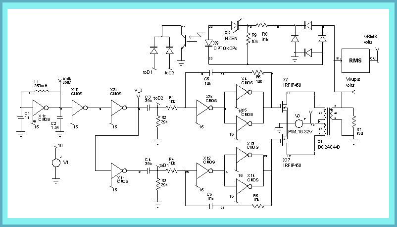
Figure 7, 400Hz push-pull inverter. The transformer was
designed and modeled with Magnetics Designer. VO supplies the
DC input voltage.
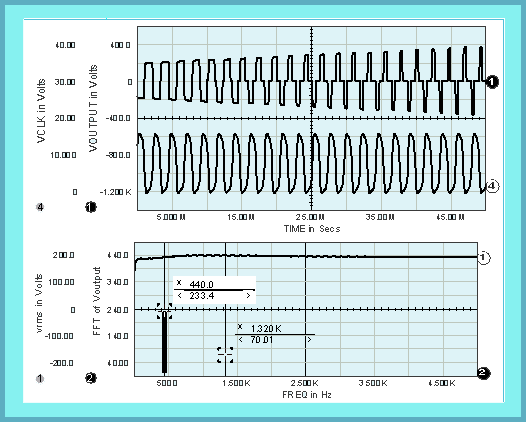
Figure 8, Plots of the output and clock signals (top graph),
the RMS value of the output (lower plot, waveform 1), and the
output frequency response. As the FFT of the output shows, even
harmonics are suppressed.
The transformer design and SPICE model was created with Magnetics Designer. The following specifications were entered:
| Input Specifications | Synthesized Design Results | ||||||||
| Operating Frequency: | 440Hz | Core Loss | 1.959 (Watts) | ||||||
| Core Family/Material | EI Lamination 6mil Square | Copper Loss | 5.464 (Watts) | ||||||
| Temperature rise above ambient | 35 degrees C | Weight | 2.014 | (Core Weight: 1.228, Copper Weight: 0.7856, in pounds) | |||||
| #1p | #2s | #3p | #1p | #2s |
|
||||
| Voltage per winding | 62 | 880 | 62 | Turns of wire | 57 | 810 |
|
||
| AC RMS current per winding | 3.4 | 350m | 3.4 | Wire Gauge | 19 | 29 |
|
||
The digital gates were modeled at the transistor level. They could have been modeled with digital gates, but the close ties to the analog elements would have required several A-D and D-A bridges (8 total) which in themselves can increase circuit complexity. In the end, the complexity is approximately equal. ICAP/4 includes digital gates modeled at the transistor level and at the gate level, so users can have a choice of which approach to take depending upon the ratio of digital to analog circuit content.
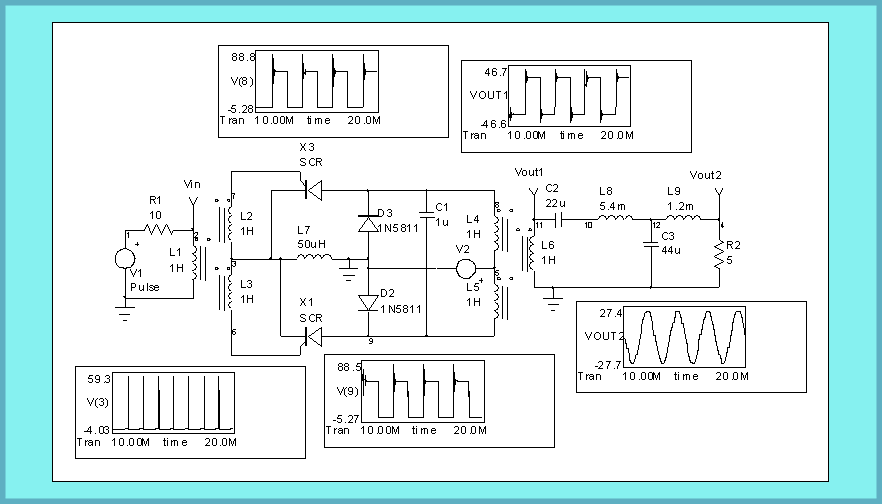
Figure 9, A 400Hz SCR inverter.
400Hz SCR Inverter
One of the major applications for SCRs is converting DC to AC power in the kilowatt range. Again, high efficiency is an important feature. For supply voltages above 24Vdc, values greater than 90% may be obtained. To avoid unilateral saturation of the output transformer and to make use of the full dynamic range of the magnetic material, a parallel inverter configuration is used to deliver symmetrical square waves under all load conditions (Figure 9). All odd harmonics are cancelled by the push-pull mode of operation. Feedback diodes prevent the voltage across the primary windings from exceeding the supply voltage.
Because SCRs cannot be turned off by their gate signal, a return to the blocking state has to be forced by reversing the anode voltage. Commutation is initiated by turning on the nonconducting SCR. For a small period of time, both SCRs are conducting. To avoid a short circuit, a small inductance, L7, is inserted. It operates as a choke by taking up the battery voltage. Finally, the conducting SCR is turned off by the negative charge that is stored in commutating capacitor C1. Values of C1 and L7 depend upon the supply voltage, the SCR recovery time (10-20µs) and the current to be commutated.
To get an undistorted sine wave output, a wave shaping filter has been added to eliminate all harmonics in the square wave voltage. The transfer function of the filter is independent of the load at the fundamental frequency.
Rload=1 to 10Zo (equals 5 here), Zo=3W, fo=400Hz, C2=1/(12pfoZo)=22u,
C3=1/(6pfoZo)=44u, L8=4.5Zo/(2pfo)=5.4m, L9=Zo/(2pfo)=1.2m. Additionally,
the filter presents a capacitive input impedance to the SCRs to
support commutation.
BACK
TO THE TOP
For the novice, and sometimes well seasoned SPICE users, analog simulation can present many pitfalls. In this section, we try to address some of them and provide advice and insight on how to avoid problem areas.
Ideal Elements: Parasitics
Characterizing the circuit, also known as modeling, is one of the most important aspects of simulation. Modeling issues pervade the entire simulation process. Therefore, it is not surprising to find pitfalls with even the most basic passive elements. In most schematic packages, placing a resistor, capacitor or inductor inserts an ideal version of the element. This means that there are no parasitics included.
Fortunately, such parasitics aren't usually critical to the design performance. Well, at least you hope you've designed your circuit to be parasitic intolerant. But as far as the simulation accuracy is concerned, it's up to you to determine where you want to add complexity in terms of element parasitics.
R-L-C Component Frequency Spectrum Limitations
Electronic circuits are always modeled over a finite range of the electromagnetic frequency spectrum. There is really no need to describe operation of electrical components from DC through RF, to microwave and on to the optical, x-ray and gamma ray spectrum. Not only would the model be complex, it would also be inaccurate and would provide unnecessary information.
The nodal system of equations which SPICE solves are valid only when the circuit elements are small compared to the wavelength of the highest frequency of interest; this limits the high frequencies below the optical band. Even with this limitation, the useful frequency range runs from milli-hertz to many gigahertz, over 15 orders of magnitude. The reactance chart of Figure 10 shows the expected range of parasitic inductance and capacitance over this range. The darkly shaded region represents the values of impedances that are realistically achieved with common R-L-C components and printed circuit board technology.
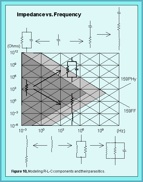
The lightly shaded region of impedances can be viewed as a transition region where parasitics become increasingly important. The boundary between the lightly shaded region and the unshaded region represents the smallest capacitance or inductance parasitic value, and therefore values in the unshaded area are unrealistic for single discrete components. At the high frequency end, this suggests the use of smaller geometry microwave integrated circuits, while extending the impedance range at lower frequencies requires larger geometries than are ordinarily found in PC Card technology.
The modeling additions for various components are shown in the pictorial inlays. First, resistors are basically defined at DC, and turn into effective capacitors or inductors, their impedance converging to that of free space divided by the square root of the dielectric constant, something in the neighborhood of 125 Ohms for PC cards. Similarly, capacitor and inductor impedances funnel toward the impedance of the propagating medium at high frequencies, and become resistive as the frequency approaches DC.
SPICE built-in models provide reasonable first order approximations for circuit behavior. Unfortunately, most circuits must be designed to be tolerant of second order effects, and sometimes to compensate in order to achieve a desired performance level. Most frequently, the parasitic and second order effects are related to changes in frequency.
The Intusoft model libraries and IsSpice4 can help determine which parasitics, if any, will affect your design performance.
|
.SUBCKT CAPACITOR1 1 2 {ESR=1M
ESL=20N RLEAK=100MEG C=???} * Parameters: C Capacitance in Farads, ESR ESR in Ohms * ESL ESL in Henries, RLEAK Leakage resistance in Ohms C1 1 3 {C} R1 3 4 {ESR} L1 4 2 {ESL} RL 1 2 {RLEAK} .ENDS .SUBCKT INDUCTOR1 1 2 {DCR=1M CP=??? L=???} * Parameters: L Inductance in Henries, DCR DC series resistance in Ohms * CP parallel capaictance in Farads L1 1 3 {L} R1 3 2 {DCR} C1 1 2 {CP} .ENDS .SUBCKT RESISTOR1 1 2 {R=1K LS=??? CP=??? TC=100U} * Parameters: * R - Resistance value in Ohms * CP - Parallel Capacitance in Farads * LS - Series Inductance in Henries * TC - Temperature coefficient in 1/degrees C, 100ppm default) C1 1 2 {Cp} R1 1 3 {R} RMOD .MODEL RMOD R TC1={TC} L1 3 2 {Ls} .ENDS |
| Figure 11, Passive component subcircuit netlists including 1st order parasitics. The parasitic values are passed into the subcircuit at runtime or left at their default values. |
Subcircuit based models can hide the parasitics, while parameter passing gives you the freedom to specify their values. The nonideal passive element subcircuits, shown in Figure 11, are included in all ICAP/4 packages. Note: Sophisticated models for tantalum and ceramic capacitors were covered in newsletters #44 (Nov. '95) and #45 (Feb '96) (Past issues of the newsletter are available from Intusoft).